 This article will explore how the Starlink REV3 (a.k.a. G3/V3) power architecture is implemented.
We will learn how the Starlink “PoE” is implemented and how the Starlink board powers up.
This information might be helpful for those doing Starlink repairs.
The primary focus will be on the rev3 boards, which are the most common worldwide (as of summer 2024).
Please let me know if you want a similar article for other revisions of the terminal.
Warning: A lot of pictures are below.
Starlink PoE implementation
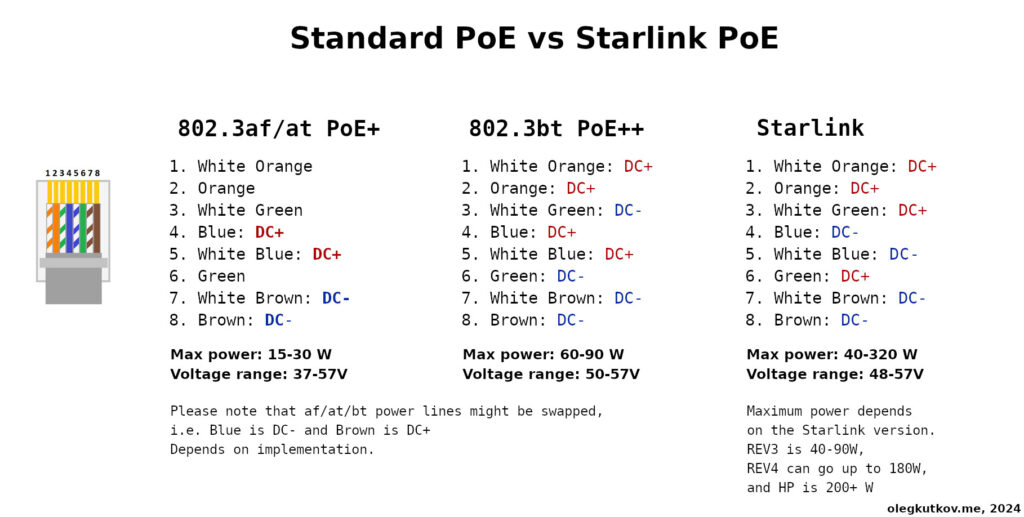
All Starlink terminals (except MINI) are powered via the Ethernet data cable, which implements the proprietary Power Over Ethernet standard.
Voltages range in the cable from 48-56V, and the power is 45-320W, depending on the terminal model.
Please note that the Starlink PoE is incompatible with any PoE standard, such as PoE+ or PoE++. The power line pinout is different.
Besides, there are no PoE standards for such high-power devices.
Connecting any standard and dumb PoE injector might damage your Starlink or PoE injector. Always use PoE injectors designed for Starlink, such as Yaosheng or DishyPowa.
Most PoE standards typically implement some detection and classification of the connected devices. The Power Sourcing Equipment (PSE) controller sends a sensing voltage and detects the connected Powered Device (PD) response. This helps to negotiate safe voltage and power when it’s needed. You can read more about PoE detection/classification here.
Starlink is no exception but implements its own PoE signature and detection. A custom controller and detection circuits are in charge.
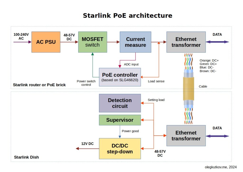 Here is the PoE circuit in the Gen 2 Starlink router.
Starlink PoE controller
This is quite an unusual chip.
The controller IC is SLG46620 – “GreenPAK” Programmable Mixed-signal Matrix from Renesas. This is a small CPLD-like chip, a one-time programmed microcontroller. SpaceX created and preprogrammed the design once, and now Renesas is producing these ICs. This is why you can’t google and replace this chip with something else.
Burned-in logic is quite simple: apply test voltage, measure consumption, enable main power MOSFET, measure consumption, and cut the voltage in case of trouble. Repeat.
This IC is used in the REV1/REV2 PoE brick (both for the router and the Dishy), HP, and the GEN2 router. They replaced it in the GEN3 router with an STM32 MCU.
The sense voltage is 2.7V for the GEN2 router and 4.4V for the REV1/REV2 PoE brick.
The trigger load on the line is <= 3.2K. When such resistance is measured between the Ethernet power pairs, the controller activates the power MOSFET. The REV1/REV2 PoE brick also checks for shorts between orange-to-green and blue-to-brown pairs, meaning all four lines are connected.
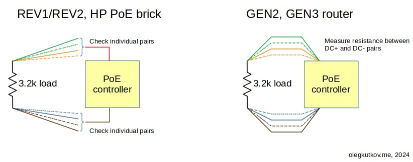
The PoE controller activates the main power for 876 ms and measures current consumption. If the consumption is not sufficient (the line load is no longer 3.2k), the controller cuts the power and sleeps for 450 ms. Then, the cycle is repeated.
Please note there is no handshake and complex verification from the terminal side. It will start when the appropriate voltage is applied to the line.
So, why non-standard PoE?
When the first Starlink terminal came out (in 2020), Dishy’s total power consumption was 180W.
The REV3’s power consumption was significantly reduced to 40W (non-heating mode). However, the current REV4 is also power-hungry.
HP Dishy can jump up to 300W, which is enormous.
There is no PoE standard for such high power. The best PoE++ can provide up to 90W.
SpaceX had to develop its own “standard” with all safety features.
REV1 and HP Dishes also use custom thicker Ethernet cables to provide enough power over the long cable.
Besides, Starlink does not use “PoE” or “Power Over Ethernet” phrases in its documents, labels, and even code.
Starlink REV3 architecture
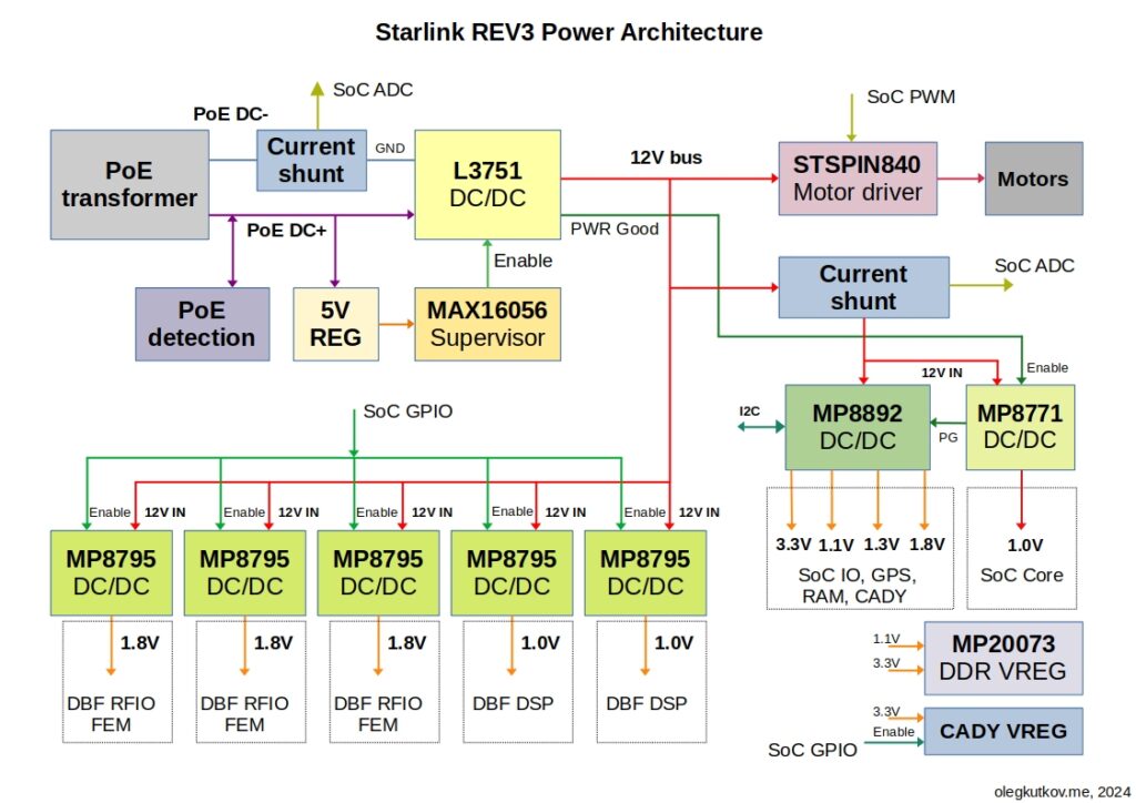
Below, you can see the power architecture diagram for the REV3 terminal. Other revisions are somehow similar, but we are focusing on the REV3.
Brief description
Input PoE voltage is dropped down to 12V and then distributed across various voltage regulators.
These voltage regulators provide different voltages for the SoC, antenna array, GNSS, and other consumers. This is generally true for every Starlink revision.
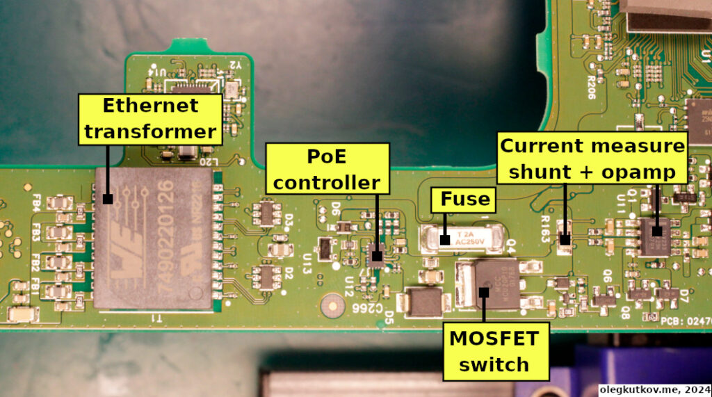
The Input PoE current is controlled by the shunt and operational amplifier connected between the PoE return line (DC—) and the board’s GND.
The PoE detection circuit generates an initial power consumption signature, which the power supply uses to activate the main power.
The primary voltage regulator is L3751, which has a wide input range. This regulator drops the input PoE voltage to 12V, the primary internal voltage. Alternatively, they use LM5146, which is practically the same IC with the same pinout.
The MAX16056 power supervisor controls the primary regulator operation. The supervisor circuit implements input voltage monitoring and generates some delay for the L3751 enable pin. L3751, in turn, generates a Power Good signal, which is used for the SoC voltage regulator activation.
Starlink SoC with peripherals requires different voltages to operate. The MP8771 regulator generates 1V for the CPU cores.
Power Good output of the MP8771 activates Enable input of the MP8892. The MP8892 is much more complex and generates four voltages:
– 1.8V for the SoC IO module and GNSS receiver.
– 3.3V for the system clock generator (CADY) and GNSS receiver.
– 1.1V and 1.3V are also for the SoC, RAM, and GNSS receiver.
This 4-rail voltage regulator is connected to the SoC via the I2C bus and provides monitoring and regulation (AVS).
The MP20073 is a highly specialized regulator required by the DDR RAM.
The CADY clock generator section requires a 3.3V and ENABLE signal from the SoC’s GPIO. This section has three linear voltage regulators, which will be described below.
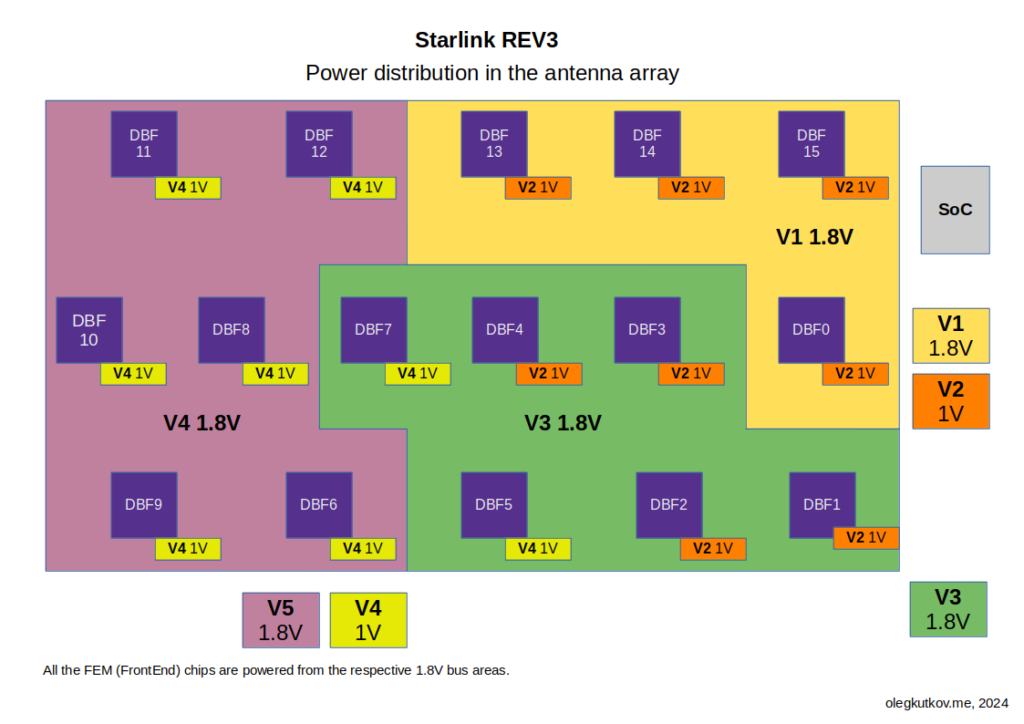
Five MP8795 voltage regulators provide power for the whole antenna array. All 16 Digital Beam Former (DBF) ICs with their Front End Modules (FEM) are getting power from these voltage regulators.
Two MP8795 generate 1V for the DBF digital section (DSP cores)—eight DBF ICs per regulator. Three MP8795 generate 1.8V for the DBF IO and FEM ICs. One regulator powers 10 DBF ICs with corresponding FEMs. The second regulator powers ten more. The third regulator powers the other four ICs.
Components placements on the PCB:
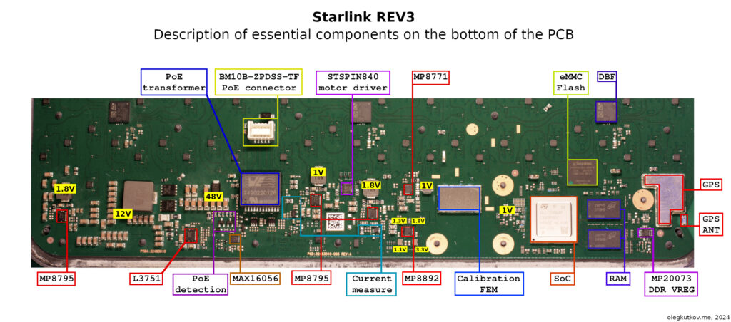 Click on the image to see the full-resolution version
 Click on the image to see the full-resolution version
Modules description
Now that we’ve got the big picture let’s dive into the details of each module.
Input connector, Ethernet transformer, and PoE input
The input connector type is BM10B-ZPDSS-TF(LF)(SN). The cable side is ZDPR-10V-S.
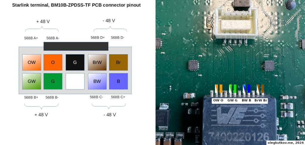
Below, you can see the connector pinout (PCB side) and how the lines are routed to the PoE transformer. This info can be helpful if the connector is torn off the board.
The PoE transformer is 802.3bt-rated 7490220126 from Wurth Elektronik, but it’s hard to find. Possible replacements are 749022013 or WA8704-ALD.
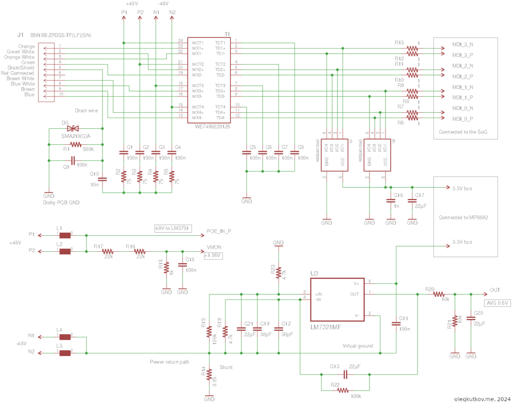
Complete schematic of the input section:
The input section is a typical Ethernet/PoE circuit with the PoE transformer, Bob Smith termination, and protection elements.
The drain wire from the data cable is connected to the Dishy GND via a paralleled capacitor, resistor, and TVS diode.
The capacitor creates a low-impedance path for high-frequency noise. The 500k resistor helps drain any extra DC, effectively limiting the current in a normal situation. TVS diode SMAJ10 helps in extreme conditions, quickly draining any high-voltage spikes.
Ethernet lines are protected with two WE824015043 TVS arrays. There is no separate Ethernet PHY. Data lines are connected directly to the SoC.
The power lines are taken from the corresponding Ethernet pairs as described above.
There is also a slight tap in the form of a voltage divider, which monitors the input voltage.
The negative (return) line is connected to the GND via the 0.05R shunt. The LM7321MF amplifier measures the current across the shunt. This amplifier has a single power and “virtual” ground separated from the primary GND with the shunt. Additional components are required to create a frequency response and provide filtering before feeding the output voltage to an ADC input.
PoE detection
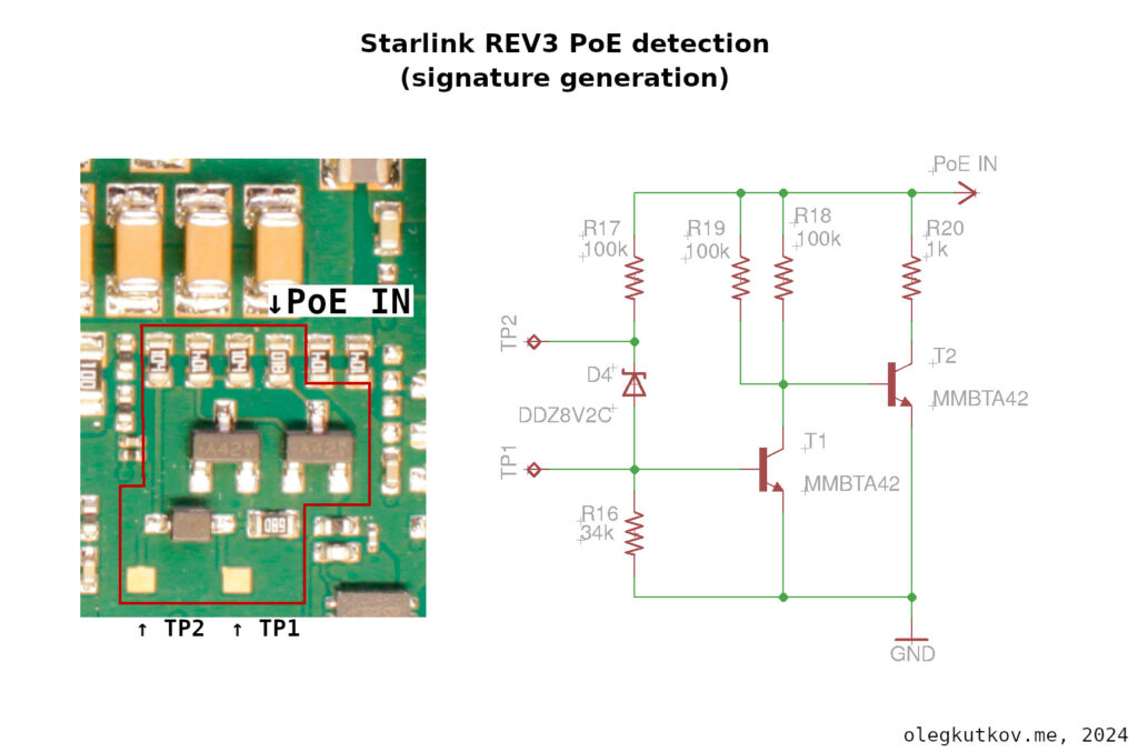
The PoE detection circuit is quite simple. It’s connected directly to the input 48V rail (PoE transformer) and generates the required signature for the power supply unit.
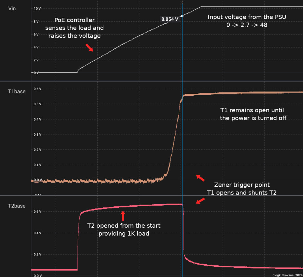
When the router’s sense voltage (2.7V) is applied to the PoE input, T2 immediately opens with the help of two 100k resistors connected to the base. T1 is closed, and the T2 base is not being shunted. The opened transistor loads the line with the 1K resistor. This value, plus some resistance from the cable, creates enough load to trigger the PoE controller in the Starlink router or Starlink power brick.
The voltage starts to rise, and when it reaches approximately 8.5V, the current starts flowing via the DDZ8V2C zener diode and eventually opens T1. This transistor shunts the T2 and disconnects the 1K load from the line. This happens quickly enough (less than 400 microseconds) to save the 1K resistor from overheating.
The power line remains active for 876 ms. This is enough time for the primary voltage regulator to kick in and consume power instead of the 1K resistor.
T1 remains open so that parasitic current consumption will be less than 0.00096A. This can be neglected.
MAX16056 supervisor
The primary purpose of the MAX16056 is the soft start of the L3751 when the power is stabilized.
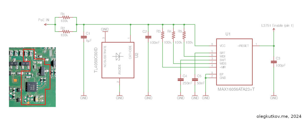
The supervisor IC is powered directly from the input PoE line via current-limiting resistors and 5V TL4050 shunt voltage reference.
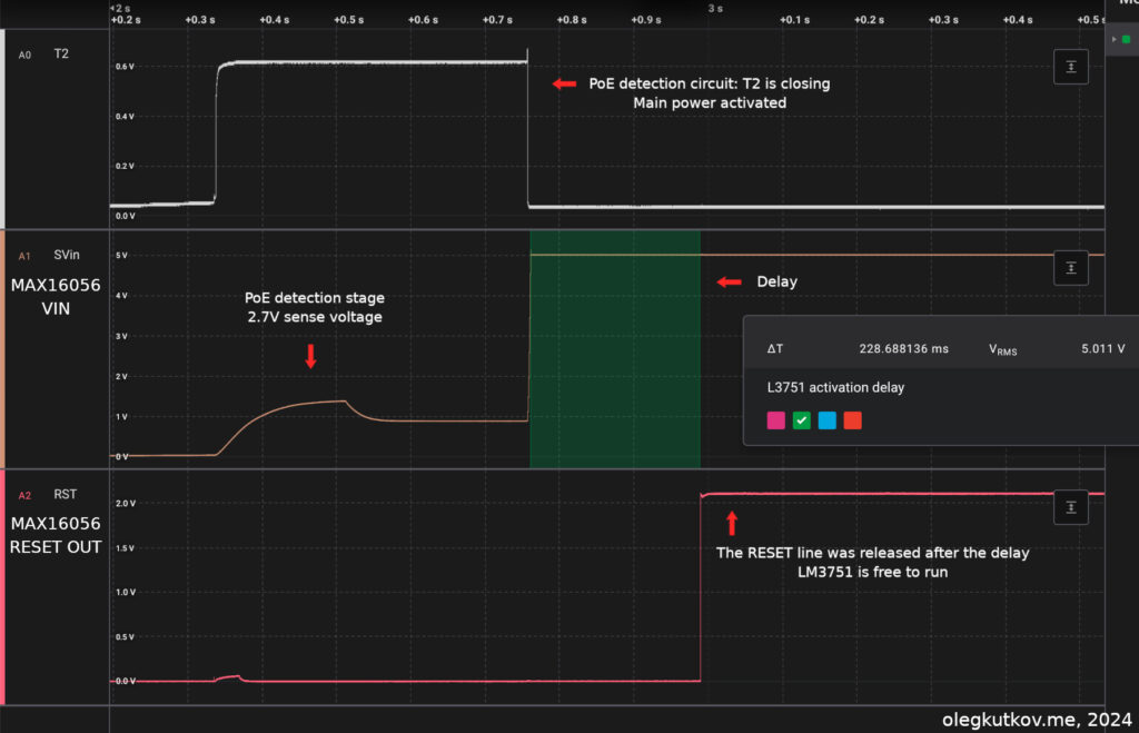
With a series of resistors and capacitors, the MAX16056 is configured for a 229 ms RESET line delay.
The RESET line is pulled down on start, disabling the LM3751 voltage regulator, and released when the timer elapses (229 ms).
This creates a descent start delay for the primary voltage regulator but still fits into the power activation cycle (876 ms).
L3751 primary voltage regulator
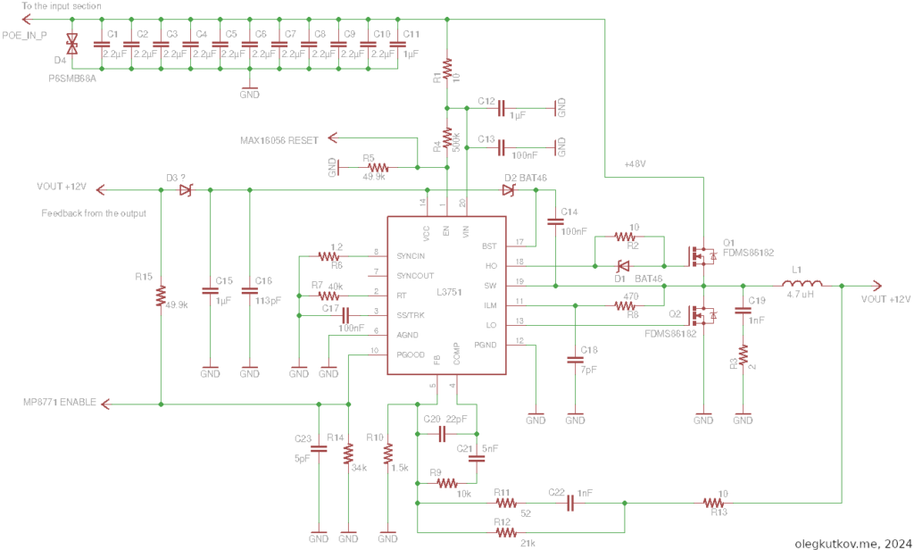
48V from the input section connected to the array of capacitors and additional TVS diode. This array helps compensate for losses in long cables during peak power consumption.
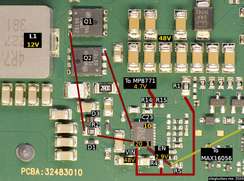
LM3751 is powered (VIN) via a small current limiting resistor from the input line. Two resistors on EN input form a voltage divider. This helps to activate the voltage regulator only when the input voltage is higher than a specific low limit. The minimum required voltage on the EN input is >1.2V. In this case, LM3751 will run with an input voltage higher than 38V. You can replace this voltage divider and make it run from lower voltages.
As described above, the EN input is also connected to the MAX16056 supervisor.
The PGOD pin directly drives the MP8771 EN input. When everything is good, this line should have 4.7V.
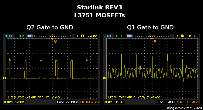
Two power MOSFETs are FDMS86182. The switching frequency is 250 KHz. The output voltage should be between 11.8 and 12V.
You can check how everything is placed on the PCB and interconnected in the messy picture below:
Here are the measurements of MOSFET gates for reference.
All measures are referenced to the GND. The Q1 high-side looks unusual with a higher Vpp because it’s not directly referenced to GND and is powered via the D2-C14 bootstrap circuit.
MP8771 core voltage regulator
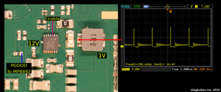
The following primary voltage regulator to start after the L3751 is MP8771. This regulator provides a single 0.9-1V voltage for the SoC CPU cores.
PCB layout and essential signals:
MP8892 4-rail voltage regulator
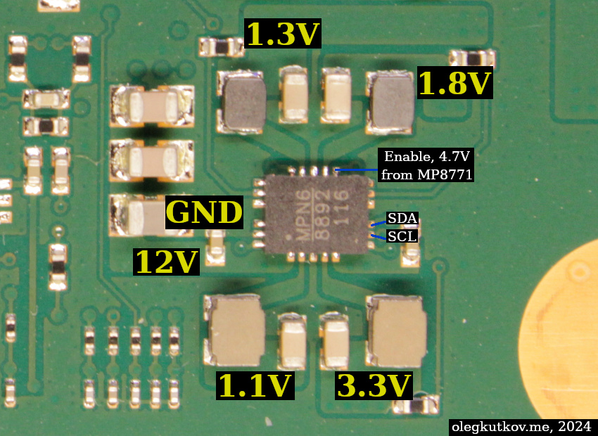
MP8771 from the previous step activates MP8892 when everything is good. The MP8892 provides four voltages for the Clock module, GNSS, DDR RAM, and SoC IO module.
Unfortunately, there is no datasheet available for this chip. An additional reverse engineering is required.
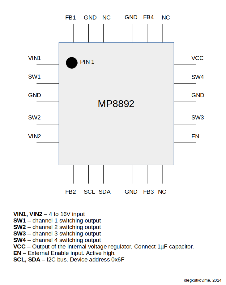
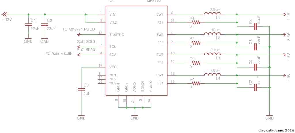
The MP8892 is a complete power management IC (PMIC) integrating four high-efficiency, step-down DC/DC converters and a control interface (I2C). The voltage regulator provides up to 4.5A (single line) of current. The switching frequency is 1MHz, so the output inductors are pretty small.
The output voltages can be adjusted through the I2C bus or preset by the three-time, multiple-time programmable (MTP) memory e-fuse. In the case of Starlink, preprogrammed voltages are 3.3, 1.8, 1.3, and 1.1 V. The regulator always starts with these voltages.
MP8892 pinout:
Schematic is very simple:
PCB layout:
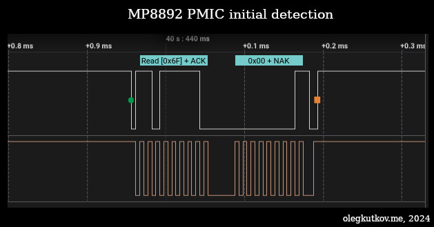
MP8892 is connected to the SoC I2C-3 bus for configuration and monitoring. The device address is 0x6F. The registers map is unknown since there is no public datasheet. Starlink firmware executing i2cdetect command on boot: i2cdetect -y -r 3 0x6f 0x6f
This is how it explained in the firmware code:
On some UTs, the PMIC only responds after querying it via i2cdetect with read byte commands for probing. It is unknown why.
Nothing in the datasheet suggests this is needed.
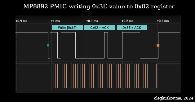
Next, the code writes a specific value (0x3E) to register 0x02. It might be some voltage profile selection.
Most likely, there will be some additional writing and adjustments during runtime.
MP8795 and antenna array
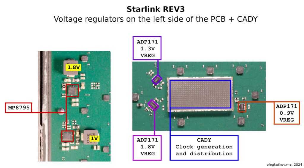
Five MP8795 provides power for the antenna array. Three 1.8V voltages are provided for the RF front chips and DBF RF IO, and two 1V voltages are provided for DBF DSP cores. All voltage regulators are activated from the software (SoC GPIO) when the terminal is booted.
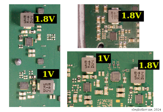 Here is how the power from these voltage regulators is distributed:
The 1.8V rails are for the DBF chips’ analog part (RF IO) and front-end elements (PA + LNA), and the 1V rails are for the DBF digital cores (DSP).
MP8795 V1 provides 1.8V for the DBF0, DBF15, DBF14, and DBF13 chips and all surrounding small FEM chips.
V2 provides 1V for the DBF15, DBF0, DBF1, DBF2, DBF3, DBF14, DBF13, and DBF4.
V3 provides 1.8V for the DBF1, DBF2, DBF3, DBF4, DBF5, DBF7, and all surrounding FEM chips.
V4 provides 1.8V for the DBF5, DBF7, DBF6, DBF9, DBF10, DBF8, DBF11, DBF12 and corresponding FEM chips.
V5 provides 1V for the last eight beamformers’ DSP cores: DBF6, DBF9, DBF10, DBF8, DBF11 and DBF12.
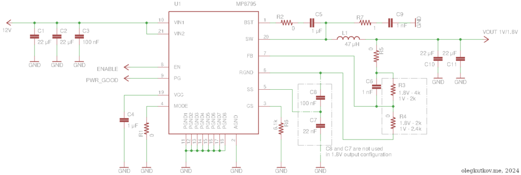
All five MP8795 regulators are implemented similarly, except for the feedback circuit. Two resistors define the output voltage.
In the 1.8V configuration, the R3 value is 4k, and the R4 value is 2k. In the 1V configuration, the R3 value is 2k, and the R4 value is 2.4k.
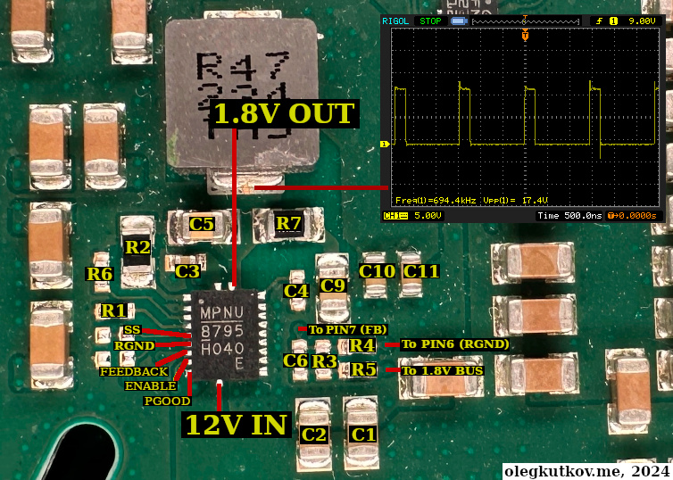
Additionally, the 1V variant has two capacitors for the soft start option, which is also implemented for the 1.8V regulator on some Starlink boards. There is no rev/pcba difference between these two versions (w/ 1.8V and w/o soft start).
Below is the PCB layout of one of the MP8795 regulators (left 1.8V). All components were marked according to the schematic.
Digital Beamformers and FrontEnd Elements
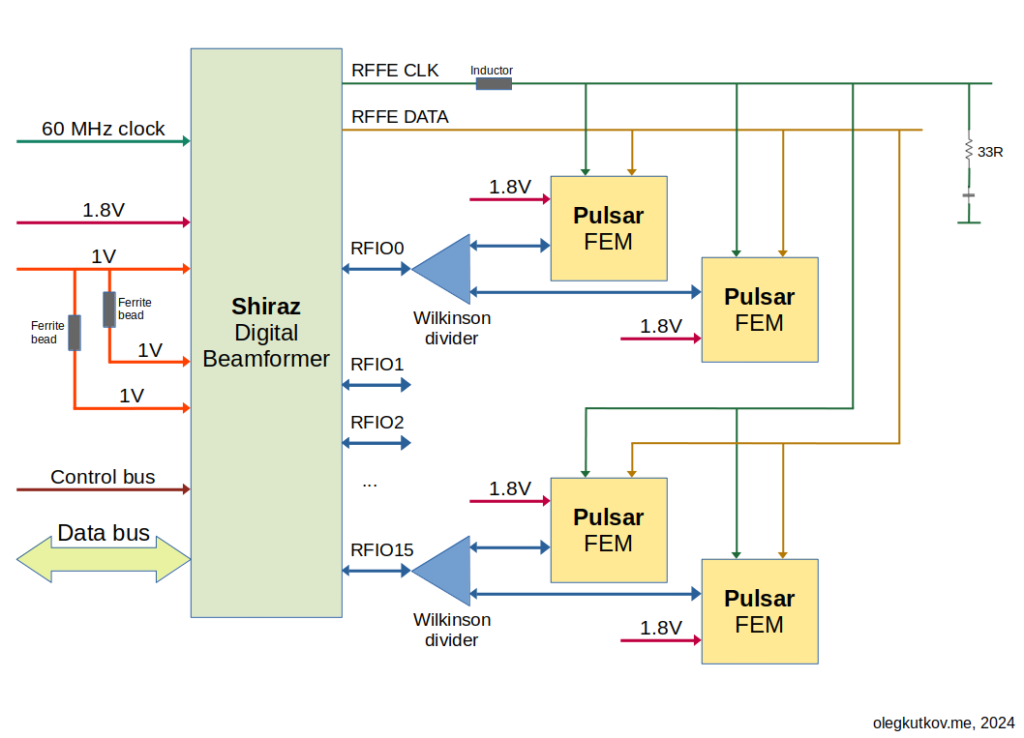
Beamformers and RF architecture are outside the scope of this article, but we will examine the general architecture, power bus, and crucial signal distribution.
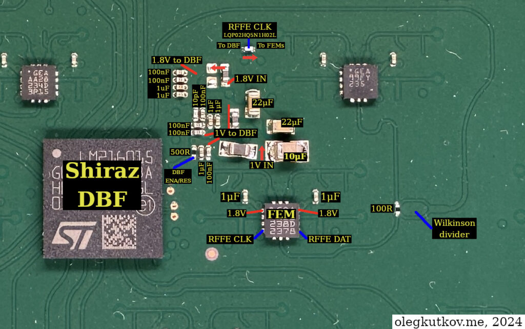
Beamformer IC (codename – Shiraz) requires 1V for the DSP core and 1.8V for the RF IO.
The 1V line is split into three lines to provide power for different submodules of the Shiraz chip. Two 1V lines have additional filtering and bypass capacitors.
Each beamformer has 16 RFIO channels and 32 associated FrontEnd Modules (FEM, codename – Pulsar). Each FEM contains LNA and PA, plus an additional analog phase shifter. Thus, two patch antennas (for TX and RX) are connected to the single FEM. All FEMs are powered by the 1.8V bus. There are separate power inputs for the LNA and PA sections.
Additionally, there is a serial two-wires control bus (RFFE) between the beamformer and associated FEMs. RFFE clock line is terminated with a 33 ohm resistor.
DBF, FEM, and power lines PCB layout:
CADY clock generation and distribution
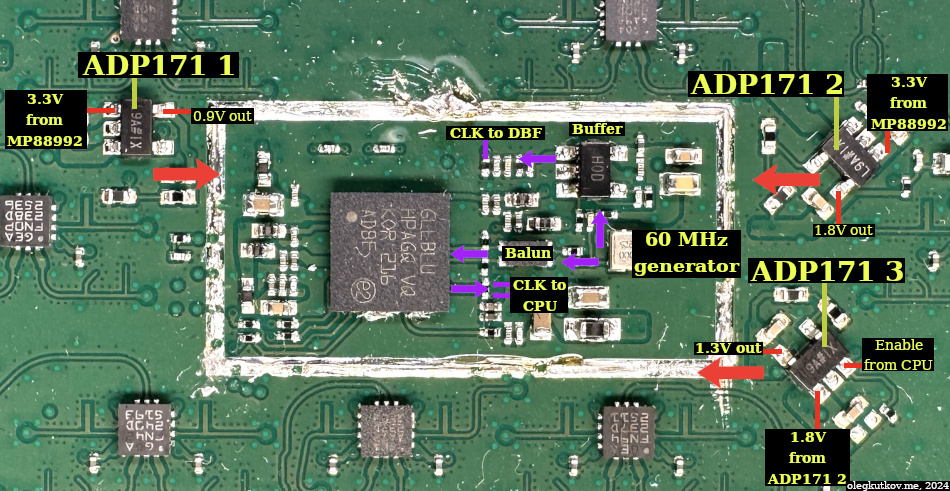
The CADY section is simple and contains a 60 MHz crystal generator, buffers, and differential amplifier.
The 60 MHz clock drives DBF chips (single-ended line) and the SoC (differential line). This module starts on power-on and provides the crucial clock for the SoC.
Additionally, the firmware activates some of the CADY components on boot.
SoC
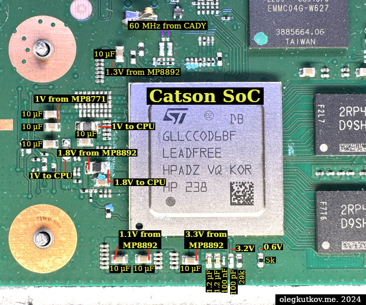
The Starlink SoC’s codename is Catson (REV1-REV4). This article does not provide a detailed description of this chip. We will focus on essential power lines.
The power supply system is relatively standard, with many bypass capacitors. The capacity of most of the smaller capacitors is 100 nanofarads.
60 MHz voltage level is 0.4V (to GND).
Starlink motors and motors driver
Starlink drive motors are creatively repurposed motors from car folding mirror drives. They are regular brushed DC motors, 12V, with a typical consumption of about 0.4A.
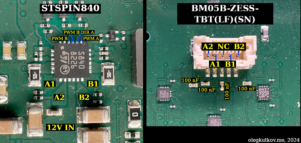
A dual-channel DC motor driver, STSPIN840, controls these motors. The motor driver is controlled with PWM signals from the SoC and software. It provides feedback about motor consumption so the software will know when motors are stuck or reach extreme positions.
PCB socket is BM05B-ZESS-TBT(LF)(SN). The cable connector is ZER-05V-S.
Common Problems and Solutions
Problem: Starlink is not Starting, and there is no voltage on the PoE input connector.
Solution: Check the router/PoE injector. Check the state of the Starlink cable and proprietary connectors.
Problem: There is a constant low voltage on the PoE input.
Solution: Check the main voltage fuse inside the router or PoE injector. Check the state of the PoE detection circuit. Damaged resistors might prevent T2 from opening and loading the line.
Problem: PoE input voltage is jumping between low and high levels.
Solution: The Starlink is most likely not consuming power. Check that the 12V is not shorted. Check that MP3751 is starting and that the voltage on pin 1 (ENABLE) is present.
Problem: PoE input voltage jumps between low and high levels, and the primary inductor makes a clicking noise.
Solution: The 12V bus is shorted. Check all the voltage regulators. Remove the MP3751 inductor and apply voltage to the 12V using an external power supply. Set the power supply to 3V and maximum current. Next, find the overheating section.
Problem: Starlink is starting. The Starlink App always shows a “booting” state.
Solution: Install the Star Debug app from a marketplace and check the Dish tab and Ready States section. Most likely, some of the MP8795 is not working. Check all 1 and 1.8 voltages.
Problem: Starlink is starting, and Star Debug shows only RF failure. All 1 and 1.8 voltages are present.
Solution: Some of the Pulsar FEMs are not starting and most likely shorting the RFFE bus. Check resistance on the RFFE clock and DATA lines on each DBF section. Use a high-resolution multimeter to find the chip shorting the bus. Replace the faulted chip.
Problem: Starlink is starting. The Starlink App always shows a “booting” state; all modules are green.
Solution: Check the GPS state. Starlink will be stuck in the “booting” mode if there is no valid GPS signal. If necessary, replace or rework the STA8089 GNNS chip.
Thank you for reading. I hope this material will help you repair the REV3 Starlink terminal.



Hello Oleg, congratulations on the blog, it has changed the lives of many people here in Brazil.. antenna turns on and keeps looking for satellite and doesn’t come out of it.
Hello. What’s in debug data?
weak signal
I have the voltages in the 1.1 and 1.8v clock 60mhz converters
in the stardebug snr app it is false
in the stardebug gps app it is valid
I have uplink
and I don’t have downlik on the graphs below
weak signal
Hi , there is some way to bypass the restriction of 250knot for my stalink mini in an small airplane? Thanks a lot
Hi Oleg, Thank you for such an excellent analysis of Starlink Rev 3 / Ver 2. Your work is exceptionally detailed and well thought out, and it is extremely helpful. Congratulations with much respect and admiration for your work!
One question – do you have a similar analysis for Rev 4 / Gen 3 non-articulated dish?
Hello! Not yet, but I will do. Such a work requires some time.
Sorry, meant to say Rev 3 / Gen 2
hey, really interested in the calibration fem module, how it works? for which signal path?
Hello. This module is similar to other FEMs on the PCB, but the output of this module is connected to a test pad. On previous terminals, there was a SMA connector.
SpaceX use this module to test and calibrate Starlink terminal at the factory.
ok, is it designed for the rf calibration, connecting the output pad to the testing antenna?
and also, there is an through line on the antenna printed layer, is it also for tesing and calibation?
Hello, my starlink was damaged in a storm. The casing cracked. It worked normally until the rain came. When the water got into the casing it stopped working and now it won’t start. Where could I start looking for the fault? Thanks
Hello. First, clean the bottom part of the PCB (power input section) with alcohol.
Then, you can start with PoE detection section. Check that the detection voltage is applied and that this section triggers the main voltage activation.
If everything is Ok – check the L3751 VIN and EN inputs. Damaged R1 resistor is common problem.
Hi. Star debug shows RF frontend error. Everything else is OK. All 1.8V and 1V around beamformers are fine. None of the RFFE lines are shorted. How can I debug this further preferrably without buying multi-thousand dollar rf measurement equipment? What is the reason of starlink showing rf front end error? I mean how is the soc able to make this assumption? Does it try to communicate with EBFs and can’t do that or what?
1.8V for FEM power is toggling on and off with a period of ~5 seconds – this is the startlink doing multiple attempts to start-up the RF subsystem I assume. Eventually it gives up and 1.8V is permanently on. Also on the “Power distribution in the antenna array” image the green section drops to 600mV when it’s regulator is OFF. Other sections drop to 0v. Is this normal or maybe it’s a hint to whats wrong?
> this is the startlink doing multiple attempts to start-up the RF subsystem
Yes. The firmware applies 1.8V and then asks FEMs status from each DBF.
There is a retry counter for this procedure.
Hello.
> Does it try to communicate with DBFs
Yes. The firmware communicates with each DBF chip and inquires about its status.
Next, each DBF is responsible to it’s FEM chips. It attempts to enumerate each FEM and sends and reads calibration data using the RFFE bus.
If an issue occurs, DBF reports an “RF” issue to the firmware.
If something is wrong with DBF(s) and it’s not responding, we are getting “AAP” error.
Unfortunately, we can’t read the detailed error status, which can point us to the specific DBF/RFFE section.
There are several approaches to the RF error. You can hook up an oscilloscope to each DFB’s RFFE bus. This bus operates at a relatively low speed, so you will be able to see the clock and data pulses. If the bus is silent, here is your problematic section. Then you can try to determine which FEM on this bus is causing problems.
You can use an IR camera to find which FEM is colder (not starting) or overheating (which is most likely).
Hello, thanks a lot for your reply. I have already aquired a thermal camera and was also thinking of building a crude RFFE analyzer using some FPGA eval board. But just checking if there is communication at all would be a more logical first step. Can you confirm that RFFE communication between FEM and DBF is bidirectional? From what I measured – all FEM chips (within single DBF section) share the same RFFE bus and there is no circuitry that would distinguish one FEM from the other. How can DBF address a single FEM chip then? Maybe they have a factory-set bus ID or something?
> Can you confirm that RFFE communication between FEM and DBF is bidirectional
Yes, there are read and write commands.
There is a complex enumeration technique that utilizes broadcast commands. In general, DBF doesn’t care how many FEMs are on the bus. It will try to count all of them.
What can trigger the DBF RF error:
– Shorted RFFE bus
– No FEMs detected
– Calibration issues
About calibration. There are special calibration RF sequences that the antenna array both sends and listens to at the same time. This happens at the start. But this operation is almost impossible to fail. There should be something wrong with the antennas themselves.
hallo om oleg, saya menemukan tegangan 1,8v di pin 13 ic 8892 turun jauh dari yg semestinya, hanya terukur 4,2mv saja
kira-kira ini permasalahan nya diimana ?
Hello. The primary consumer of this voltage is GPS chip. Also, it might be failure of the 8892 itself.
Please check the resistance on this bus. If it’s to low – try to remove the GPS chip and test again.
dan tegangan 1,8v out pada pin ic 8795 juga tidak ada tegangan
8795 is activated by the firmware after successful boot.
Terminal can’t boot without the 1.8V from 8892. Thus, there will be no voltage on 8795.
Hi, starlink app shows searching satellite, and star debug shows Ready States all green, RF ready:30sec GPS valid:58,cbut First CPlane:-1, First PoP ping:-1. And all 1.8v and 1v are good. So what is the possible issue?
Hello. What is the version of the firmware?
2025.03.28.mr52463.2 and star debug red dot Cause: NO_SCHEDULE. I did not connect the motors cable when I powered it on. I suspect that is the reason for the issue. But even when it worked normally, it only points staright up toward the sky almost no angle.
I’m interested in the Pulsar FEM chips. Do you have any info on the serial control data to those chips? Do the FEM chips include any phase shifting, or is it all done in the Shiraz chip? Or Is it just T/R and/or polarity select?
The FEM chip includes PA/LNA switch and limited phase shifting. Additional phase shifting is performed inside the Shiraz chip.
Control protocol RFFE, but the commands are unknown. This protocol includes a quirky enumeration method.
Excellent work, I’m very impressed with your reverse engineering skills and detailed explanations.
In some of your videos you show powering a Gen 2 Rev 3 50V dishy using Gen 1 Rev1/2 56V power supply. Is this OK?
Yes, you can use gen1 power supply to power any Starlink terminal (except for HP)
Hello. Yes, 56V is totally ok.
Thank you Oleg Kutkov. This is more than great work. I’ve acquired more knowledge in the past 24hrs than I would’ve in one year on my own about the starlink Rev3(V2) power architecture.
I have a challenge. I have this kit that doesn’t connect to the router. But base on the power rails ever voltage is available except for the 1.8v and 1.0v on the MP8795s. I hope someone could help.
Здравствуйте, Олег! Хочу уточнить по взаимозаменяемости чипов DBF. Возможно ли установить данный чип с другой антенны? Есть несколько плат, но отличаются маркировки на чипах DBF. Разводка на платах визуально одинаковая. Имеют ли данные чипы адресацию, т.е. для замены можно использовать любой DBF чип или тот, что установлен в конкретном месте? Спасибо.
Добрый день. Если чип с платы такой же ревизии то можно. Они между собой взаимозаменяемые. Адресация там динамическая, так что все подхватится.
Problem: Starlink is not Starting, and there is no voltage on the PoE input connector.
My Problem is ON dish cable connector 8 pin at WO, O , has 2.8 V
miss 48V . Please Help How to Solve. Thanks You,
Router Power Supply out put has 48V and 12 V.
Олег, цей пост просто клас, дозолив мені за вихідні оживити (по живленню) 3 тарілки, від яких відмовились в майстернях. Мені здається що в розділі MAX16056 можна вказати, що там MAX16058ATA з open-drain (ну в V3 в мене) якщо я все правильно прорахував. Для таких як я зекономиш купу часу 😊 . В MP8771 я знайшов r5, який під’єднаний попереду l1, а не за.
Головне питання, звідки у куди приєднані 0,6V і 3.2V в картинці SoC? (ну одна частина в самому SoC на піні знайдено, а друга?)
Зі знятим SoC зараз 0(V), поки стояв на платі показував 1.7(приблизно) замість 3.2 і якісь мілівольти замість 0.6. По цих вольтажах, можна казати, що CORE дихає, чи вже всьо?
Друге, якщо б ти в двох реченнях вказав би як знаходити коротиша в RFFE (де які перемички) і пробиті FEM, то хлопці були б щасливі ).
Як на мене ти провів мега роботу!
0,6V – це напевно VREF/VTT DDR, формується самим SoC. Залишилось 3.2V. Хоч куди дивитись? Окрім покупки нового ))
Hello, how are you… I have a Rev 3 (V2) antenna which started malfunctioning after a hailstorm (I should mention that the casing didn’t break and no water got in). It works fine for a while, but then the signal cuts out. When I opened it, I didn’t find anything unusual at first glance, but the 4R7 coil gets extremely hot — to the point that it starts heating up the board. Has anyone had this problem? Thanks in advance.
Boa tarde, consigo usar na G3 ?, um poe de 12voltss, esse poe é no padrão starlink.
No caso ao inves desse poe mandar 48v, ele só mandaria 12v, e tudo pelo cabo de rede mesmo.
I have a problem with a circuit ESD protection
Wait, the P47 isn’t receiving power for pins 1.1 and 18. Meanwhile, the 8892 is receiving power for pins 1.1, 1.3, 1.8, and 3.3. It’s all there. If it sits for a bit, it starts working, but only for about two minutes, then the power goes out.