 A few years ago, I wrote about the powerful DC motor driver based on IR2110. This construction appeared to be quite popular.
This time I want to describe a much compact and simpler (but still very powerful) solution
with IRS2104.
This device can be used to control any power-hungry DC load like DC motors, heaters, and so on.
Like IR2110, the IRS2104 is a high voltage, high-speed power MOSFET and IGBT driver. The new IC provides much simpler control with a single PWM input. Internal schematic provides protection against SHOOT-THROUGH and dead time management.
IRS2104 Functional Block Diagram
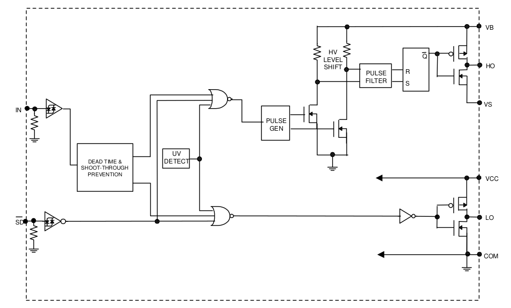
As you can see, there is only one input that allows driving the whole half-bridge. SD pin allows to shut down the output. This adds more flexibility and safety.
IRS2104 is operational up to 625 volts. But recommended maximum voltage is 600. This fits most of the applications. You can get the full datasheet here.
All basic principles are the same. You can use the previous article as a reference. The logic input is compatible with standard CMOS or LSTTL output, down to 3.3 V logic. You will need only a few extra components for the “bootstrap” circuit and so on.
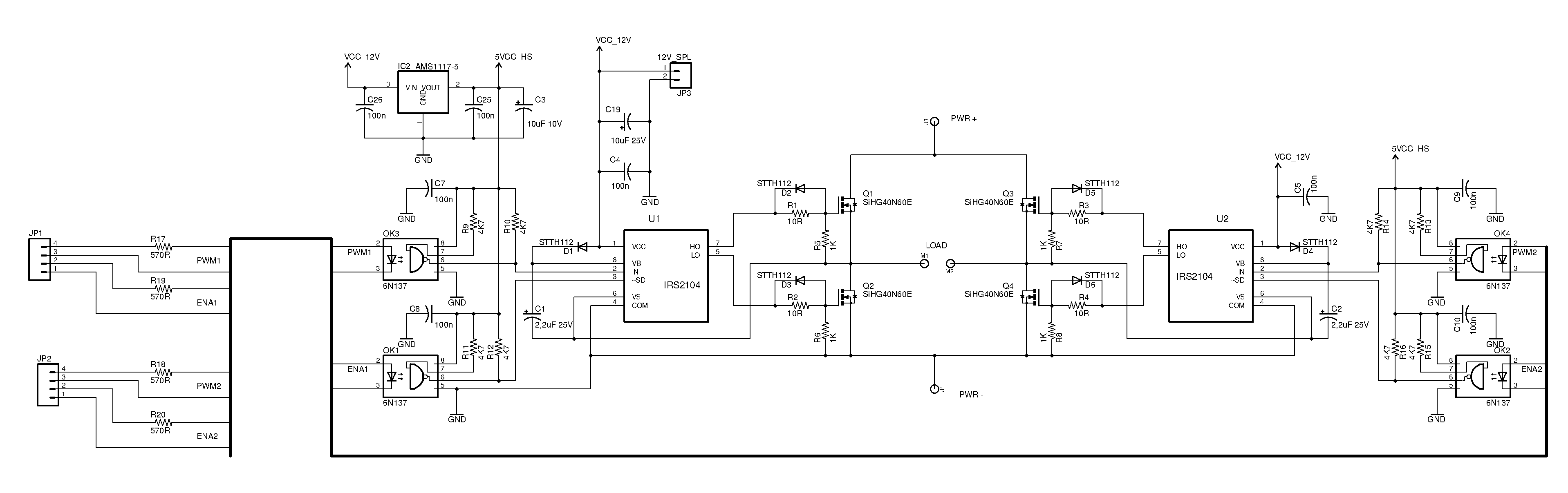
A proposed schematic implements the full H-bridge with two IRS2104.
 Click on the image for the full resolution.
The schematic is quite simple. The low voltage side is powered from the single 12v supply. All inputs are isolated with high-speed optocouplers.
You can see that SD input is also designed for the external controls. Sure, you can remove these additional optocouplers if you don’t need the shutdown control.
The selected MOSFETs can drive a 40 amps load at 600 volts at normal (+25 Celsius) temperature. Please note that there are no additional protection diodes. This means that this circuit can safely drive only low-inductance load. If you wish to drive some inductive load (like a powerful motor or some load with long connection wires) – you need to add high-speed protection diodes. Those diodes can be soldered directly to the PCB, across the MOSFETs, or placed on a separate protection board.
Please select appropriate diodes (max current and voltage).
C1 and C2 are tantalum capacitors.
The two-sided board is designed to be compact and easy to build. Almost all components are SMD.
There are additional milling for safety at high voltage.
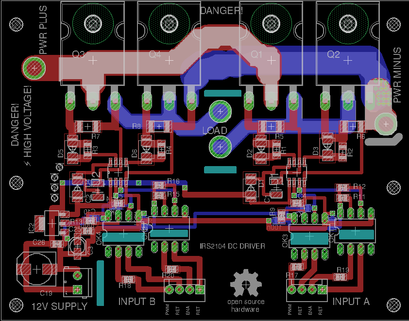
There is no solder mask on the high current lines, so additional solder can be added.
You can get the Gerber files here. Please use a thicker (> 2 mm) PCB for high-voltage applications.
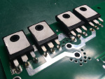
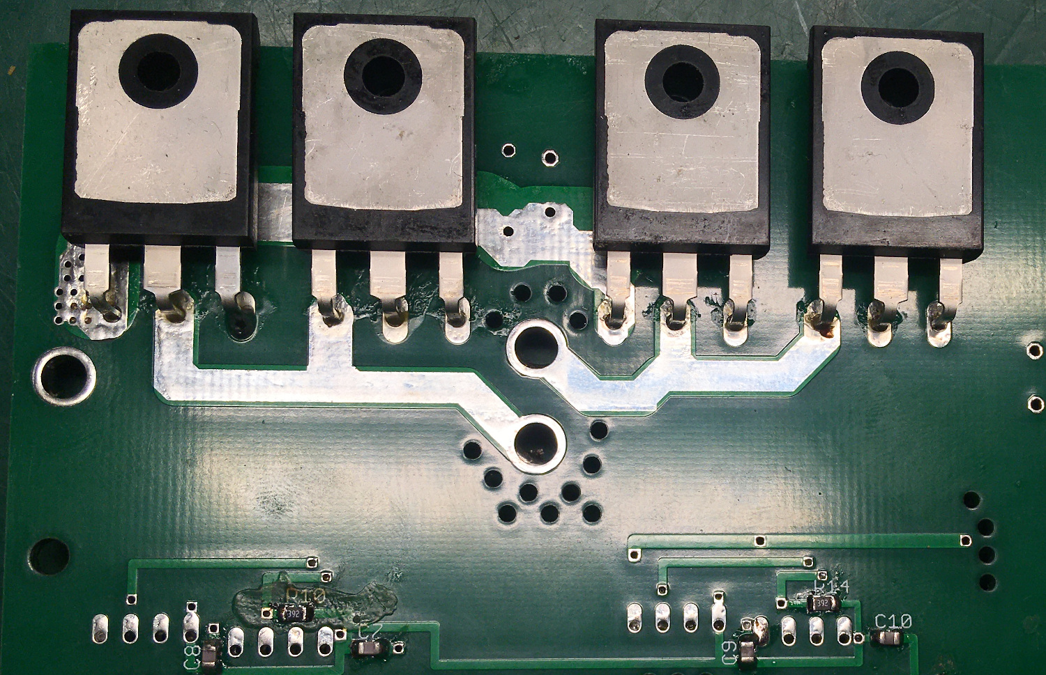
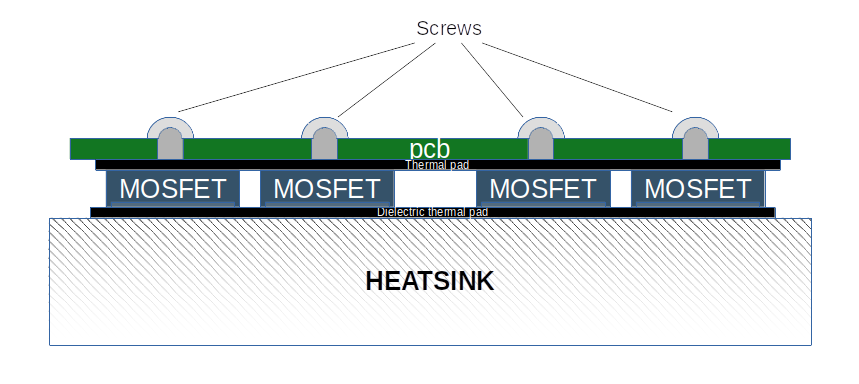
The MOSFET layout is designed to provide good contact with a heatsink in a compact environment and with minimum effort.
Possible MOSFET + heatsink layout:
 Thanks for reading!